Electrical Engineering > DISCUSSION POST > University of California, Los Angeles - EC ENGR 115Cee115c_w14_disc_wk-5_extra-problem_Solution (All)
University of California, Los Angeles - EC ENGR 115Cee115c_w14_disc_wk-5_extra-problem_Solution
Document Content and Description Below
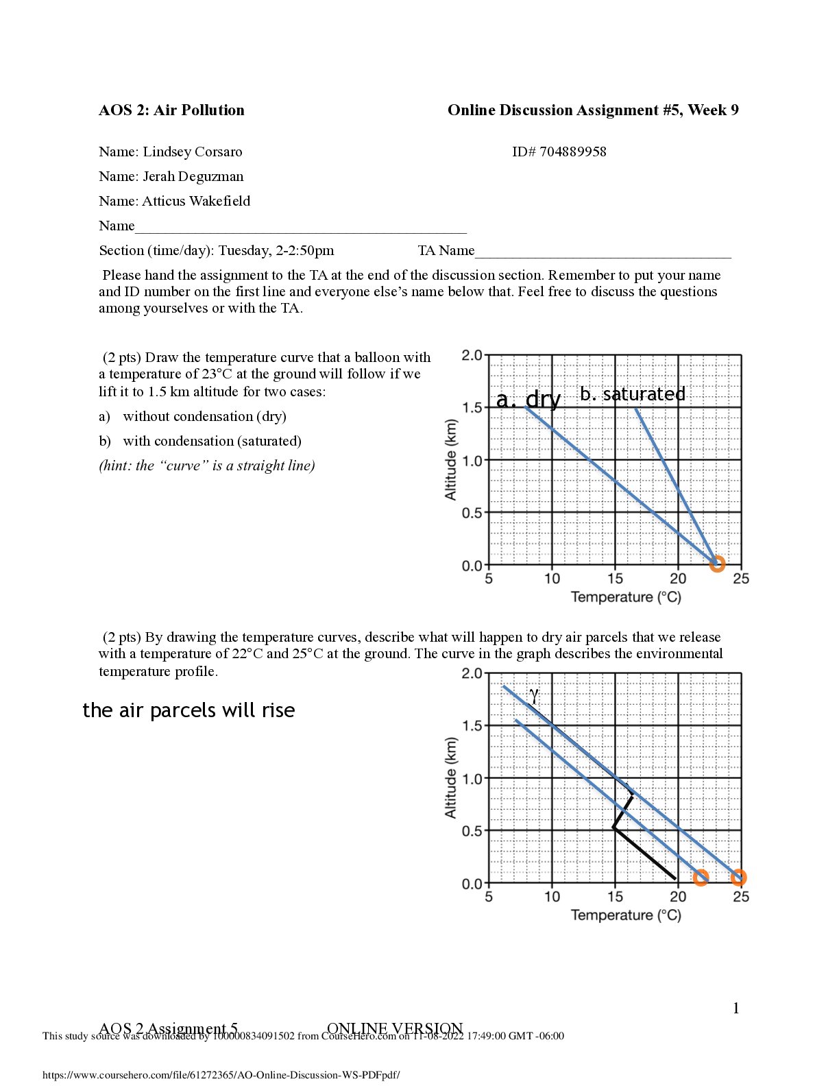
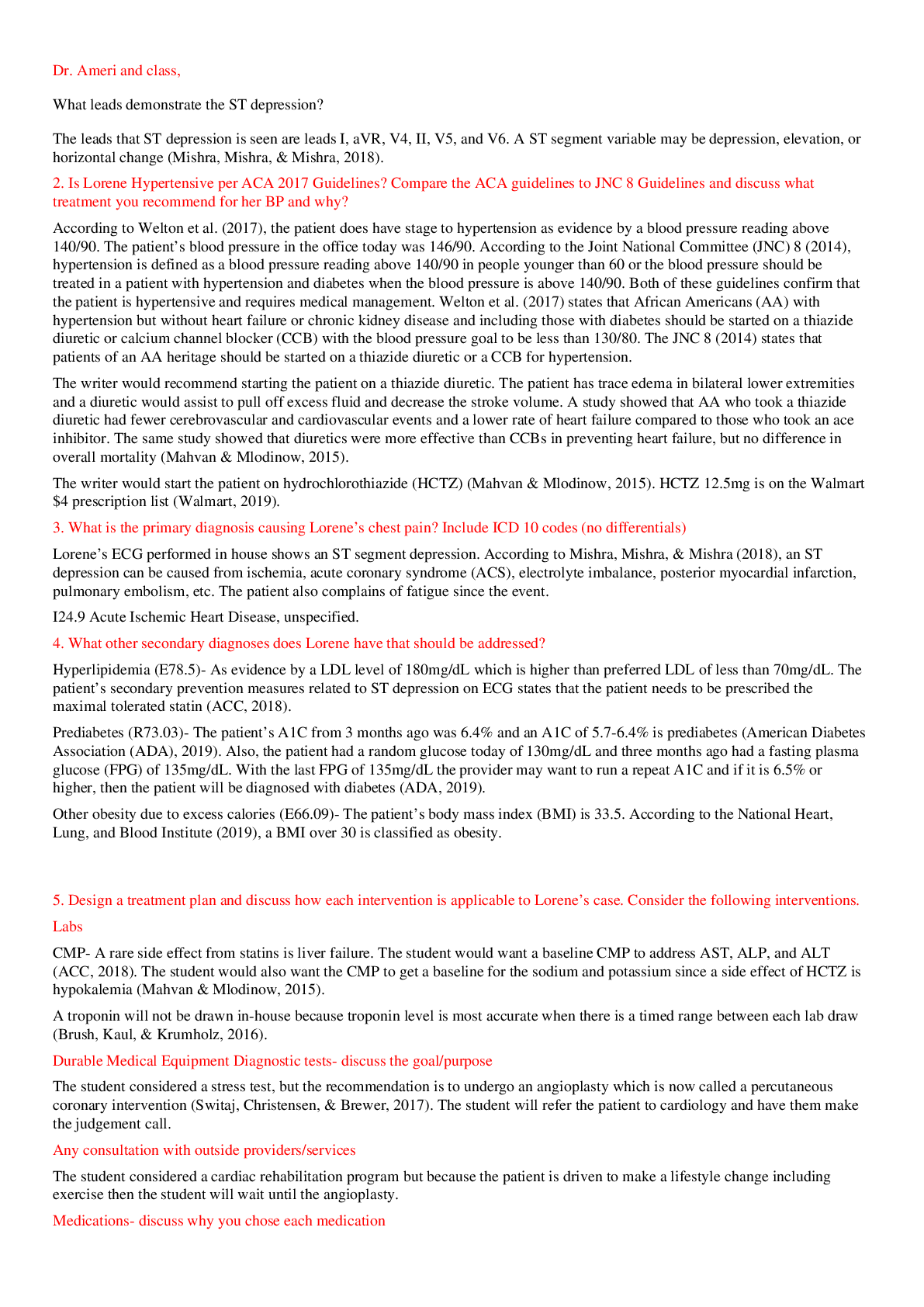
Electrical Engineering Department Winter 2014 1 EE115C: Discussion – Week 5 Solution Practice Problem 1 – CMOS Logic & Logical Effort (Previous Midterm Question) 1A Design ̅̅̅̅̅̅̅̅̅�... �̅̅̅̅̅ in Static CMOS. Draw the schematic and size all the transistors such that the worst-case delay is equal to that of a unit-sized inverter (WP:WN = 2:1). Solution: VDD Out A B C D D B C A 1 6 2 2 6 6 6 1 1B Find the logical effort for all the inputs in your design in part A? Solution: [Show More]
Last updated: 1 year ago
Preview 1 out of 3 pages

Reviews( 0 )
Document information
Connected school, study & course
About the document
Uploaded On
Mar 28, 2021
Number of pages
3
Written in

Additional information
This document has been written for:
Uploaded
Mar 28, 2021
Downloads
0
Views
27


Growth and developmental patterns of toddlers.png)